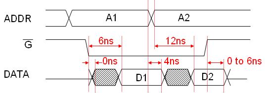

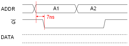
Problem 1. The Motorola MCM6264 integrated circuit is a 8Kx8 static RAM. When answering the following questions about the timing of its various signals please refer to the data sheet. Assume you are using the -12 version of the MCM6264.

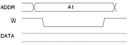
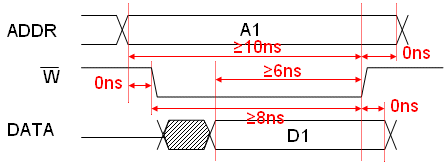
Problem 2. This problem asks you to design a memory tester that can write to memory and then read these value to validate that they were stored and read back correctly. For this problem you will be using the Motorola MCM6264 8Kx8 static RAM (data sheet).
For this problem use four address bit (assume that the higher order address bits are grounded) and four I/O pins (ignore the higher order bits). Your memory tester will write each location with its address. For example, location 4'b0010 will be written with the value 4'b0010.
Here's what the test should do:
You should take care to ensure that the timing relationships between ADDR, DATA, Wbar and Gbar meet the setup and hold time constraints mentioned in the data sheet. In particular, note that you'll want to setup the address a cycle before asserting Wbar and hold for a cycle after deasserting Wbar. It might seem that you could change the address and assert Wbar in the same cycle (after all the address has to be valid just when Wbar is asserted). However, different internal delays inside the FPGA might lead to some address bits changing just after Wbar is asserted, leading to a violation of the timing.